
It was a long and bumpy way from taking pressure transducer hardware in my hands to having stable digitized values. Most of the time I spent learning instrumentation circuitry from app notes and books, just to make sure the solution meets assumed precision despite budgetary approach. Finally constant current bridge driver, precision operational amplifier and sensitive analog-to-digital converter did a job.
For non budgetary approach semiconductor producers offer specialized integrated circuits that combine all necessary functions before reaching ADC. Using bridge driver circuit like AD623 or combination of high-precision in-amps (instrumentation amplifiers) from AD82xx series, would save my time but would instantly kill the budget as they cost from tens of dollars each. I took longer way.
First approach
Typically transducer is resistive bridge with four connections – two inputs to power it on and two differential voltage outputs. When bridge is driven correctly, the output meets specification of producer. The word correctly is a key here, as sensors are, let say, calibrated in specific conditions, usually either under constant voltage or constant current. In such conditions the producer adds extra resistors inside bridge to linearize characteristics in function of pressure as well as of temperature. From literature I found that constant current driven bridges are less susceptible to thermal deviations considering same sensor characteristics. And I ordered constant current compensated sensors from China.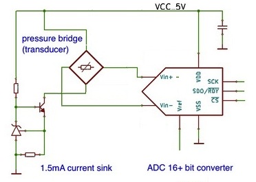
Next step was to design driver. With differential input of high-precision ADC I had freedom of choice, how to setup either current sink or source for bridge. I took as granted +5V supply, simply because most of remaining part of this module (like ADC, MCU and RS485 driver) are typically powered from +5V single rails source and I needed to have it anyway. From ADC data-sheet I found that its input is sensitive enough to be directly connected to bridge – what a relief! No extra op-amps!
Moving to current driver I was mostly interested in temperature compensation – the precise value of current was less relevant, I had to interpret voltage anyway so further calibration (real voltage to real pressure) was necessary anyway and I envisioned it will be done by microcontroller. Precision programmable voltage reference TL431 used to drive NPN transistor could work as current sink.
As the remaining part of transmitter, the MCU and RS485, looked more simpler I decided to create PCB at that stage. I have mounted current sink and ADC and started first tests. To my surprise in constant atmospheric pressure output voltage was changing a lot with temperature changes (tested in iced water and hot water). Current meter has shown current sink is not working properly, the current was changing with resistance thermal changes of pressure bridge.
Bridge driver correction
I discovered serious flaw in design reviewing ADC app note once more: it was using 300 ohm bridge while mine was nearly 3kohm. Calculation shows obvious mistake: TL431 tries to keep reference pin at 2.5V so it is emitter potential, plus 0.2V of collector-emitter in worst case (saturation) plus voltage drop on bridge when driven with 1.5mA (which is around 4.5V) that gives at least 7.2V of VCC!
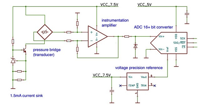
Higher supply voltage of bridge was at the maximum ratings of ADC so voltage shifting had to be added. I turned a circle around instrumentation amplifiers – I had to find cheap, zero-drift, single-rail op-amp. Having some experience with photodiode drivers I used matching op-amp as differential amplifier accompanied with precision resistors: keeping gain low (between 1 and 10) I could shift original bridge voltage span of 100mV up to 1V but in reference to ground. The remaining problem was that opamp powered from the same source as bridge (ie 7.5V) would still accidentally drive ADC input out of max range (6V). I needed protection for unexpected conditions. To avoid another op-amp I added clamping Zener diode in between – when opamp gives voltage in working range it does no affect circuitry but if accidental breach happens its clamping voltage keeps ADC input in safe range. What is more important diode junction does not generate extra noise impacting 16-bit ADC readings (in test with 21-bit ADC last 5 bits fluctuated same way with- and without clamping diode).
Second revision of construction passed in-house tests with simulated hydrostatic 1m of water pressure, thermal tests in constant pressure and deep dive in field conditions (river dam).

In-house hydrostatic pressure tower
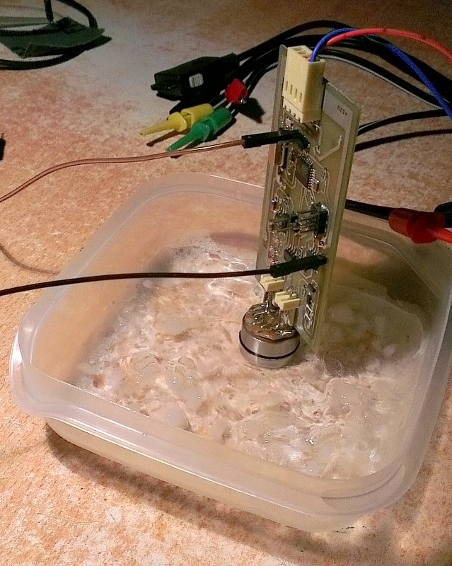
Temperature compensation tests
Bridge driver final cut
[Edit 2014-03-07] Thanks to discussion with Jose I was given a lesson on current sources and then did a homework. Voltage reference with negligible small quiescent current (micro-amperes) comparing to output current(milli-amperes) can be simply paired with resistor on output to generate constant current of value calculated from Ohm law. TL431 would not work well as its working current is around 1mA (and not guaranteed to be stable). In contrast the $1 chip REF3025 from Texas Instrument does what needed adding only 40-50uA to equation.

Primary target was not component replacement. Turning current sink to current source simplified overall design: I could remove instrumentation amplifier and clamping diode reducing this section from 12 to 3 components. As direct bridge output span is 100mV and extra 10x gain is gone, I swapped 5V reference in SOIC-8 case with 1.25V reference REF3012 in tiny SOT-23 package correcting ADC resolution as well as saved extra space.
ADC precission
Or in other words how many bits I needed. Let start with boundary conditions: measuring up to 15m of depths means 25m of full scale (atmospheric pressure is equivalent of 10m o water and adds to absolute transducer scale). To have at least 0.5cm precision it turns into 5000 steps. At the same time input from bridge uses only fraction of full scale (1/5 of scale when in-amp was used and 1/12 of scale with REF3025 as current source and 1.25V reference for ADC). That makes expected resolution order of magnitude bigger. To handle 50000 steps ADC of 16-bit is required (2^16 = 65535 values). With the MCP3550, 21-bit ADC, that I had in my inventory I could go even further to sub-millimeter scale. That could happen only in theory because:
- total error sums up, other components introduce their own errors, far beyond LSB bit of ADC,
- PCB design has to follow very rigorous rules to get beyond 16 bits – even I kept lines short and distant from noise sources I observed fluctuations of last 4-5 bits induced by wires or amplified semiconductor noise on microvolt level,
- the water surface is floating anyway, it is always averaged value, there is no reason to get far away from centimeter scale in open-water conditions.
See also other related articles:
[posts_by_tag tag=”WLS”]


Hello!
I have just discovered your very nice blog and read throughfully your series about this water level measurement design of yours! It’s a very nice design and an ever nicer educative way of sharing.
Re-reading this entry and the way you designed the bridge aconditioning subsection, I (think) found a pretty direct simplification of your design by which you can get rid of the instrumentation amplifier sitting among the bridge transducer and ADC altogether.
Assuming you have to stick with a 1.5 mA current for biasing the bridge, and that your bridge is 3K in the reference calibration point, I guess you cannot get rid of a higher than 5 volts supply for the current sink plus bridge, but you can easily remove the INA: just turn your current sink into a current source.
Moving the current sink/source to the high side means your bridge outputs will stay inside the power ADC rail, most surely for the whole measurement range (you will have to re-check on this). This way you can remove the INA altogether and reduce accordingly the BOM. You could still keep the protection L filter (resistor plus zener) at the input of the ADC, as a protection measure in case the current source fails. However, you could also do with a simple series resistor, removing the zener, as many ADC ICs include protection diodes to Vcc and so with the simple series resistor acting as a current limiter you can protect the ADC even if the current source fails.
Best regards,
Jose
P.S.: Sorry to bother you with this, maybe you already noticed and/or improved your circuit, since I have not still read all your blog entries… In any case, you can contact me at my personal email (in the form), should you want me to selflessly review any other part of the design. Peer review is still (IMHO) one of the best and oftenly overlooked engineering practices… 🙂
Jose, I appreciate your comment with detailed suggestion. This is beauty of “give a little to get a little”. As a software engineer I fully agree with peer reviews and group work but I am hobbyist disconnected from EE environment. Analogous part was most troublesome (virtually no experience here) and I stuck to datasheet note on current-sink of TL431. I could not find proven scenario with current-source e.g. mirrored circuitry with PNP on high-end (problem is Vref cannot not be used on base-emitter with that polarization)… so I hit timeout and decided to use opamp (budgetary LTC1050) and this worked in prototype 🙂 If you can share how to use TL431 on high-end as current-source I would appreciate more detailed suggestions.