
It was my first work on photo-voltaic and rechargeable batteries technology. I have read a lot about mono- and poly-crystalline cells, tracking the highest efficiency points of panels (MPPT) or proper charging/discharging. Facing that I felt I have long way to go. Until I read article on Linear’s LT3652 all-in-one chip.

LT3652 tiny case with underneath pad
Even though it was quite expensive to figure out it if fits my needs at all, I have paid $30 for two chips plus $7 for shipment from farnell.com, to get just 3rd day in the morning. I faced double challenge: firstly, I have never played with similar device and I had to design all parameters matching solar panel and battery. Secondly, the biggest size of the case is MSOP-12 that means 3x5mm layout.
While soldering 2-pins-per-millimeter was not a big deal problem was to create a PCB at home having such a thin tracks. Another barrier for hobbyist was soldering thermal pad underneath MSOP-12 case. Soldering is mandatory as I observed high thermal dissipation during the load and it is tricky on PCB without solder mask (no self-positioning of chip when heat with hot-air gun). Doing it at home definitely bumped up my soldering skills.
While designing discrete elements was time-consuming but straightforward, I faced hard time with first run. First overall estimations of power balance shown that 4Ah battery should be enough, so for milliamp current discharge, standby discharge profile is enough: that means 0.1C charging speed that turns into 0.4A. I designed maximum current closer to 500mA to charge a bit quicker in the winter when the sun is limited in my latitude. I could not pass 200mA though. What was more troublesome as the chip was getting hot scorching finger placed on it. As low current appeared at the very beginning of run it was not the thermal protection kicking in that was causing the drop. Pads size was underestimated anyway – first proto-board had only 2-3 square centimeters of copper around chip and even though it was relatively huge comparing to the chip itself it was apparently not enough.
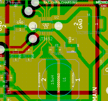
Top (red) thermal pads are not enough, bottom (green) large pad is a must.
As a next step I redesigned this board section using bottom pad having over 6.5 cm^2 plus two top-side irregular wings of extra 2 cm^2. I suspected low current is due to component missing requirements on current rush. I have shortened traces, switched capacitors to ceramic and low ESR tantalum. IC was cool now it was still far from designed current. I spent few more hours, on scope and docs, tracing why I get only half of maximum current just to learn that… the closer battery to full capacity the smaller maximum current IC uses to charge. The test preceded with couple hours of half-ampere discharge led to full throttle of charger just nicely warming PCB up. What a relief!
Next disaster I faced was circuitry protection. Application note uses Schottky diode on charger input to protect solar panel from reverse current, both on accidental connection of solar and in dark conditions to not let current flow back from battery. At the same time one of LT3652 features is maximum power (MPPT) tracking, which one of functions is to keep solar panel voltage at point of maximum current. Current changes on light conditions changes, it is obvious, and in my case does not exceed 0.7A. B140 Schottky diode 2 amps rated introduces voltage drop from 0.2 when on near-zero forward current to nearly 0.5V at 0.5A! 0.3V shift is massive comparing to other calculations like temperature compensation of photovoltaic cells introducing similar 0.3V shift on delta temp of 50*C!
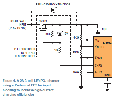
Schottky replaced with MOSFET
To deal with it I followed an article from Linear where MOSFET replaces Schottky but I found it troublesome: it relies on charging status pin I use as 3.3V MCU input to collect status data and I cannot share this pin with high voltage section. I also planned to have blocking element on low-side to share solar inpu Vin line with LM234 temperature sensor V+ pin. Neither typical MOSFET polarity protection circuit on low-end nor Schottky diode were able to save circuitry from short-circuit made by reverted battery and correctly plugged in solar panel source – few seconds of distraction during couple-hours at workbench led to tiny acrid white smoke accompanied with bunch of F-words. The boost converter diode got forward short-circuit current from battery through solar panel burning sensing resistor and Schottky diode. High current rated inductor survived but some PCB traces did not… I had no choice but introduce another home-made two-sided PCB with these clunky 2.5mm diameter vias for manual metallization.
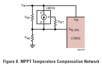
Thermo-compensation
Additional design force was to have LM234, working as temperature compensation, placed on solar panel. On schema it is placed after blocking diode and close to LT3652. To make it remote I had to make sure any cable wiring mistake will not burn circuitry again. I decided to move back to Schottky blocking diode and place it on low-end; this way V+ pin of LM234 is tied to Vin on LT3652 and has the same potential that solar input hence can be wired to positive output of solar panel next to it together with resistor, so that only one extra line goes back to LT3652 (as on schematics on the right).
To lower voltage drop on Schottky I used higher rated (3A) diode and sacrificed MPPT precision in my design, for 10 watt approach it does not really matter that much, second panel for $30 can be used if not enough power source. I also made this compensation completely optional with jumper switch on board (J8), calculating dividers with and without LM234 (the other LM234 marked U3 is for temperature compensation of VRLA battery). To prevent future accidents with polarity I have added repeatable polymer fuses on input, next to J1 header, and on battery pin, next to J7 header. Even though they are not fast-acting the reverse polarity test applied couple times proved they work fine producing significant heat but leaving circuitry working fine when correct wiring is restored.
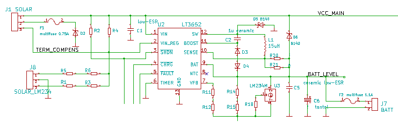
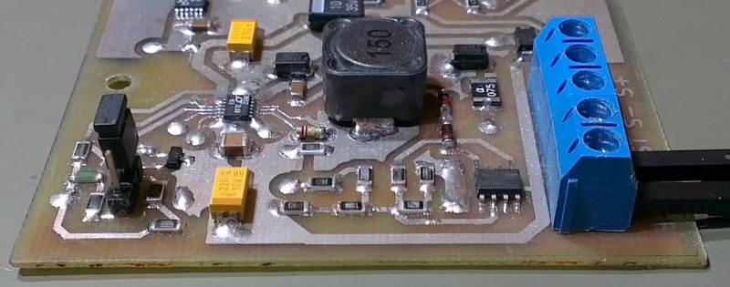
Charger part of PCB
Charger was tested during last summer (+30*C air temperature) and recent cold days (-15*C). I found that worst case is cascade of cloudy winter days combined with freezing low temperatures (halving battery effective capacity in -20*C): without direct sun charger does not kick in but to my surprise small transient current from solar (20-40mA) takes load off battery extending its work time significantly.
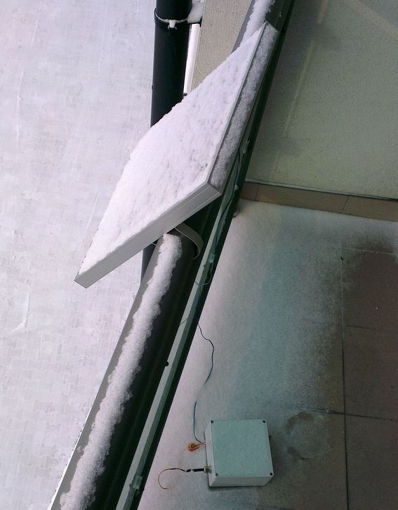
Sun blocking snow untouched, testing real conditions.
From logs I found one single series of 4 subsequent days without charging that led to 30% of battery drop at -10*C conditions, however it has never drained battery down to zero. What is also important LT3652 in MSOP12 package pinout is still in range of home-made PCBs and its range of applications makes a nice tool for hobbyist crafting either indoor charger with wide input range or typical solar MPPT-driven charger. And aliexpress.com makes it even more reachable, short series of 5 chips costs $30 with free shipment, 3 times cheaper than from farnell.com.
See also other related articles:
[posts_by_tag tag=”WLS”]


