
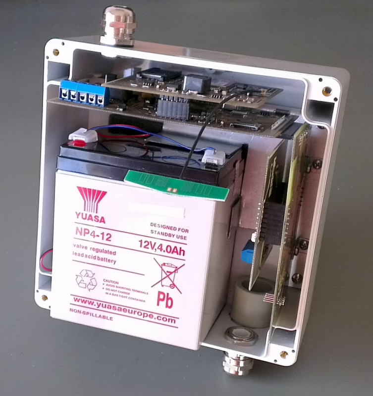
The logger part of Water Level Station experiment was second in line for design and development. The transmitter measuring water level was done first and turned to be just a warm-up comparing to logger feature list: self-powered unit with multitasking firmware, local file system and couple different local and remote buses and protocols. All that within the rigor of power and cost efficiency. Let’s take a look at the latter first.
Drawing prototype architecture of logger was easy. I had it in back of my head after series of experiments with solar charger unit, low voltage supply etc. From the beginning I predicted that most of time most modules of the system will be turned off, so the need for power switches popped up immediately.
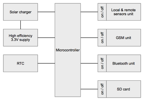
Why power off?
Remote unit current measures shown 20-25mA on 9-12V power supply level. The whole sensors unit is estimated to take up to 50mA from VRLA battery. Low duty cycle (a couple seconds of activity every couple or even tens of minutes) combined with no dedicated low-power mode made cut-off switch mandatory.

A vision by KiCAD 3D renderings
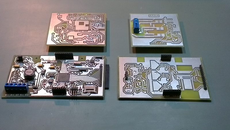
2 sided PCB prototypes, months ago
Next considered unit, the remote data transmission based on SIM900, a budgetary GSM module from China, offers multiple power saving levels: from shutdown taking as little as 20uA, through idle taking 20mA, 300-400mA transmitting data in weak signal conditions, up to 2A short bursts. As GSM unit has its own 4V switching DC-DC supply, so that battery-level current is more than halved. Power drained from battery is still significant though and never drops down to zero, even after GSM shut-down, because DC-DC supplies are ineffective in low current conditions. It was hard to predict power consumption profile and choose whether to use extra power switch or not. In case of frequent retransmissions, like every couple minutes, it would be better to keep GSM logged in to network idling in between. In contrast scenario with communication every hour or even less frequently, complete power cut-off would give more power saving on average. Since logger may have adaptive approach and changing frequency of communication I over-designed this part adding extra switch on GSM’s PSU input either.
The Bluetooth module, being a fantasy of contactless communication with handheld device (smartphone or tablet) of nearby operator, is also equipped with power switch. Reason is simple, local communication is occasional and bluetooth shutdown is its natural state.
Lastly, the SD card also is equipped with MOSFET switch. Even though it has really low power idle mode, 150uA by specification, I delegated decision to MCU, whether use power down or just rely on SD idle. Tests and measurements would show optimal approach.
High and low voltage switching
How is the switch done? It is is based on MOSFETs applied in two flavors, both with switch on high side (Vcc) as most universal approach. When the switched voltage is at the same level as driving one, like supply for 3.3V bluetooth regulated by 3.3V MCU, the P-channel MOSFET is used. Transistor turns on when low state is applied to gate node. The default state is off and is guaranteed by pullup transistor.
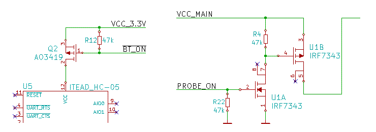
Single P-MOSFET on high side will not work for higher supply voltages, like 12-21V Vcc of GSM supply also switched by MCU. With pullup in place MCU could be damaged by way too high voltage. Without pullup in best case (3.3V on gate and Vcc on 12V) the Ugs would be still around -9V keeping switch constantly conducting. Two MOSFETS are used instead, N-channel driven by MCU voltages and turned on with its high state, and P-channel driven by the other one. In this two-transistor approach, default state is switched off by pulling down the gate of N-MOSFET.
If subsystem is capacitive load (has plenty of capacitors, especially low-ESR) then there is high inrush current when powering on. In long term exceeding maximum current can be destructive for tantalum capacitors or, in more visible manner, it can cause disrupt other systems because of supply voltage drops. For rightmost double-transistor switch there is easy way to introduce inrush current limiter by adding drain-gate capacitor of P-MOSFET (between pins 6-7 of U1B). This way gate is not immediately polarized for full-throttle but with some much lower slew-rate related to RC constant, as explained here.
Keeping costs low
Despite fundamental features constituting the logger unit with low power consumption as number one, the cost of components was second most influential factor of the design, assuming no quality degradation.
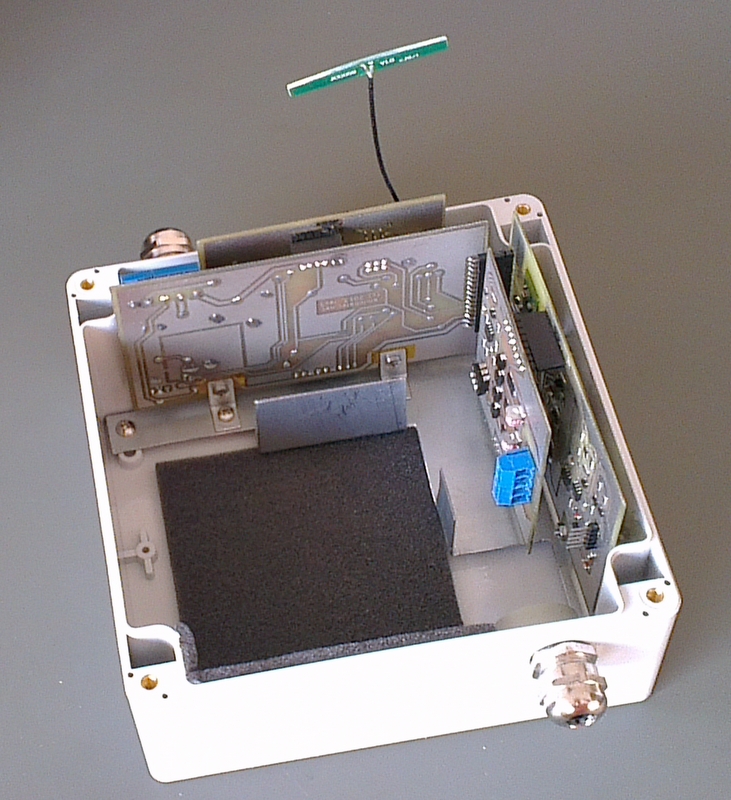
Logger case without battery
Logger case assembled
About two years ago I took the risk of importing some goods from China using aliexpress.com service. Later I started buying short series of electronic components as prices for some parts were truly competitive. And this trend continuous. The only downside is time of budgetary shipment: 3 weeks on average. If you plan ahead it pays off. Just to bring some facts, let me compare farnell.com, tme.eu or some local reseller’s prices – the SIM900 GSM module around $35 in regular stores, cheapest local reseller on auction service offers it for $25 with shipment, from China I got it for $13 (buying two for $26). The SIM900A is even cheaper, just for $10; it is two-band version of four-band SIM900 with same functionality, not available in Europe markets though. Other circuitry I was interested in I found with price halved: for instance 3.3V converter LTC3630 I paid $6 per item instead of $11, or 5V precision reference REF02 for $1.5 instead of $3.5, getting of course 10 pieces at ones. Ultimately I could get some elements at bargain prices like the strip of 100 chips of TL431 current source was for $5, while local market deals ask for it 7 times more (for the same precision and temperature range). Conclusion is obvious: careful IC choice can easily lower cost of short series production 2-3 times if going Chinese way.
See also other related articles:
[posts_by_tag tag=”WLS”]


Can I ask is that nice SIM900 KiCAD model and footprint available to download ? I have a weather station project that could use it.
Thanks.
Boards were heavily redesigned and shrinked to be made in factory, look at more recent blog entries like this one. Also first version of GSM sub-board had issues with ground loops and MCU freezing so sharing old design with flaws would not help you. As my goal is to commercialize this station one day I cannot freely share recent project files.
Hi Andy,
Just to be clear I wasn’t after the whole design, just the KiCad files that define the SIM900 component. Which is 3 elements: 1)The schematic component 2)The PCB footprint, and 3) The 3D model. In fact just the 3D model would do, I can draw the others myself but I just suck at Wings3D.
I fully understand if you still don’t want to share, it’s hard enough keeping yourself ahead with out risking things by giving away a foot hold.
Cam.
Cam, ping me back on PM you can find on “about” page to discuss what I can/can’t do for you. I am travelling far from home this week so expect delayed answer though.