
Working prototype device made of modular PCBs let me go for the next step. Learning the process of professional PCB production in factory and making short series to scale out number of devices in the field. I had to get good grasp of CAM processing, gerber files review etc. but what bothered me more was the price. With the advent of internet services for prototyping it become easier and as always Chinese had beaten the others.
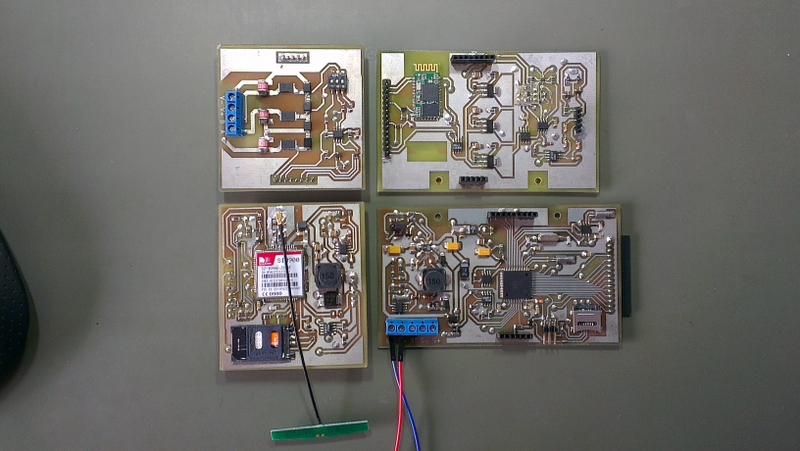
Factory made PCBs
Home made PCBs
I mastered thermal-transfer process to make PCBs at home, even for 2-sided boards: I mirror b&w image of PCB and print with laser printer on shiny paper, then I use iron pressing to stick printout to cleaned PCB, soak and remove paper, use chemicals to remove unmasked copper and later acetone to remove printer toner masking traces, voila. This approach is good for medium size of scaling down: it lacks of precision as it is hard to make thin and dense traces or small vias matching both sides of board, it does not have mask protecting from shortcuts and easing chips self-positioning when soldered with hot-air gun.
Evolution was to learn how to make professional factory-made PCBs. I had to lear all the stuff around CAM processing, how to manage all other layers never needed for thermo-transfer like silk screen or masks, how to preview produced output (gerber files) and so on. All that to make sure I get it (almost) right first time.
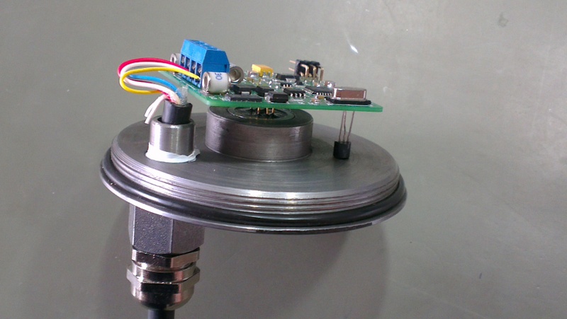
Underwater probe
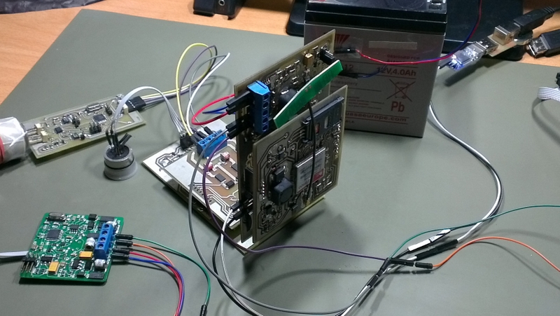
Migrating to new boards
Also looking for the right PCB fabrication service was daunting task. Most of the offline services give pricing after project files review. I did not have time for dozen of such roundtrips. From online services and forums I got at least estimates for boundaries and learnt that making one or two boards with area up to 10x10cm would cost roughly from $70 to $200 using local or European producers. To my surprise I found ITead Studio offering. That company brokers between online world-wide clients and Chinese factories integrating small designs on larger boards, subcontracting fabrication and finally reverting process cutting boards into pieces, sorting and sending back to customers. Cleaver way to get lowest possible price even for short series starting from 5 or 10 boards. Massive savings from that approach and willing to have PCBs for couple stations for field tests was perfect match instantly killing searching for anything else.
Small batch hotair soldered

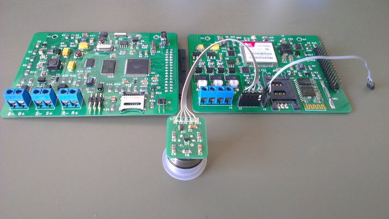
From concept to realization
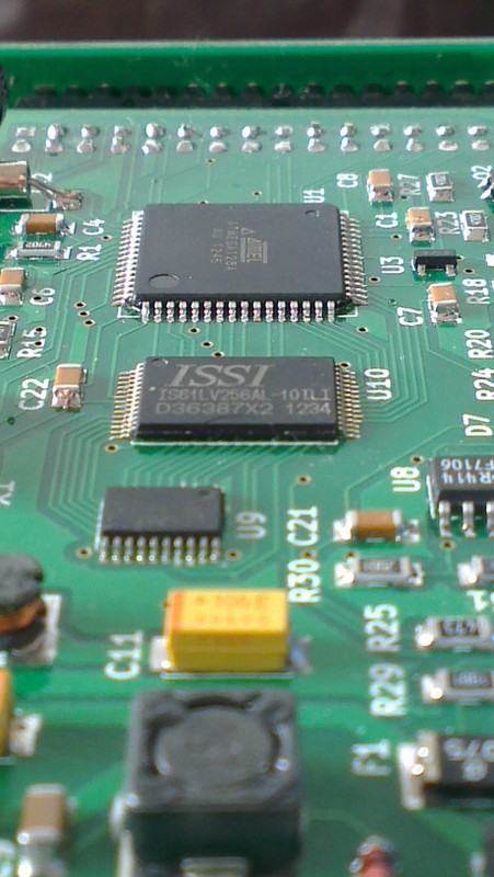
MCU with external RAM
To lower the risk of bad specification files I aimed at underwater probe PCB fist. I was able to redesign design it to fit in 5x5cm 2-sided board to match one of the ITead offers – for 10 of such boards they charge $10 plus $4 for economic shipment. In less than 3 weeks I got a batch of my PCBs. I did not use minimal parameters acceptable for fabricatino and the results were surprisingly good especially that I could find mixed opinions over the net. Maybe because my expectations were moderate, tuned down to the level matching low price. The only observable difference between gerber preview and real boards was little offset of silk screen, labels were slightly shifted, on sub-millimeter level, but pads were kept clean, not a single print on any pad.
Right after I assembled first board and run without much hassle I felt satisfaction of first professional board ever made suffering with just one minor mistake of mirrored order of pins for TO-92 temperature sensor.
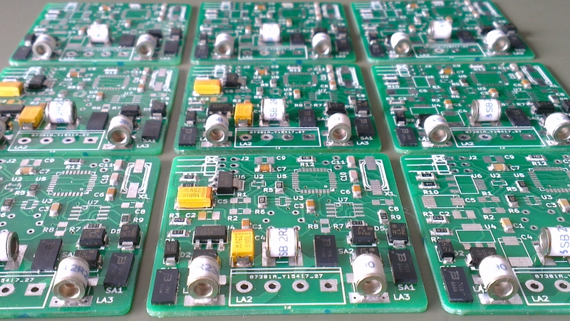
Encouraged with this milestone I jumped to redesign logger part. I knew already that I can massively shring area of boards using fraction of current values for track width, vias diameter and clearances. I decided to use nearly halve area and use 2 boards, each 10×7.5mm so that I could fit into another low budget ITead offering. To avoid any possible problems with production precisionI applied a margin (around 20%) on top of minimal parameter. Weeks later I got another short series of well produced boards, without any errors.
The only drawback I found with services like ITead was minimum batch size. For real prototyping, when board is produced to prove some ideas, any batch of size greater than 2 is simply waste of money. This problem will emerge more frequently as more and more modern chips are made in miniature pin-less forms requiring precise PCB hardly doable at home. Time will tell how market will respond to this demand.
See also other related articles:
[posts_by_tag tag=”WLS”]


