
Thanks to Chinese providers printed circuit board fabrication has never been so cheap. With PCB comparison tool it is also darn easy to choose from. Sometimes though old’ye home made PCB is what you are looking for. So I made a photostory from my one-hour creation process for newbies.
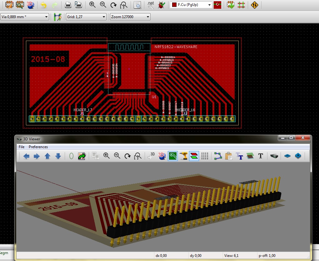
If you have $15-25 spare, then within coupla days some Chinese factory will fabricate prototype 25-50 cm^2 boards for you and over next 2-3 weeks deliver to you. All that with precision far beyond in-house process. There is a catch though: at least 5 to 10 boards must be ordered. Waste of material and money when you need exactly one board without highly packed layout, large enough traces and vias, usually without coating and labels (solder mask and silk screen). Like when you are about to use just it one time while discovering or prototyping some functionality. And that was my case: creating a breakout board for single nRF51822 BLE 4.0 chip and wire it on lager breadboard.
The whole process from opening PCB design to stage ready for soldering took me less than 60 minutes, including pauses for taking pictures. Larger number of drills or 2-sided PCB would double or triple that time.
1. PCB design
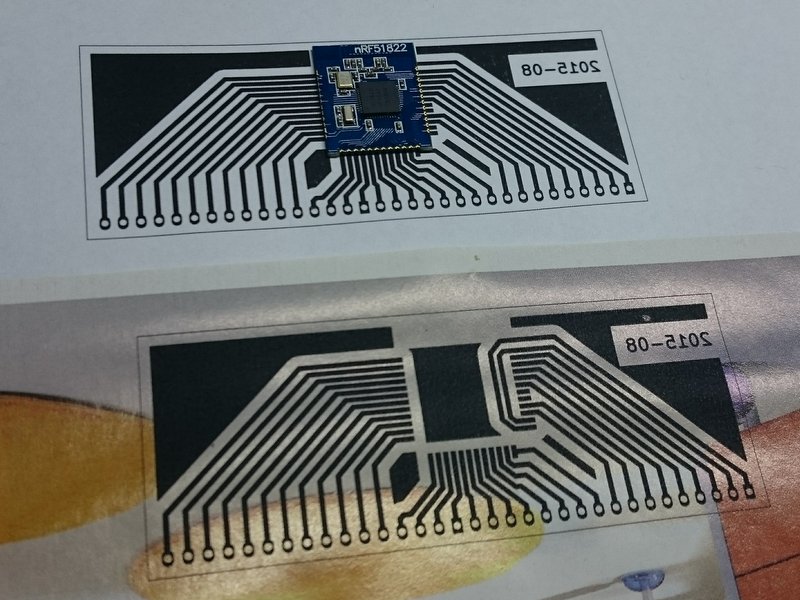
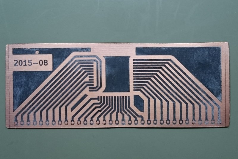
While designing for home-made PCB I keep trace width no less than 0.8mm/~30mils (occasionally down to 0.5mm/~20mils ). That gives me a margin for errors in case toner does not stick to board perfectly (see step 6) so that etching could erode edges of trace, narrowing it or breaking the contact. When PCB board design is ready I export only copper elements to SVG: silk screen, solder mask etc are set invisible.
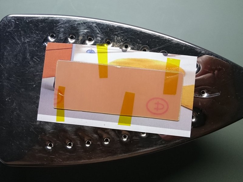
2. laser printing
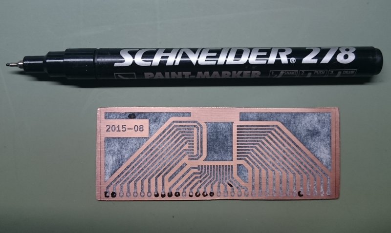
The traces on image must be mirrored, either during SVG export or later before printing. If you have top and bottom layers (tru hole design or 2-sided PCB) note that bottom layer SVG is already correctly mirrored. Design must be printed on laser printer as toner will be thermically transfered to board, ink will not work. In GIMP I open new document in A4 format, grayscale, 1200dpi (highest resolution supported by printer you have). DPI specification is crucial for details: lesser than 600dpi and thin diagonal traces will become zigzags. SVG is imported with the same DPI as my page for proper scaling. Print on thinest chalk paper (like Ikea’s catalogue); printer toner must not integrate with paper. Match components (chips, boards) with pads to check if printout is valid.
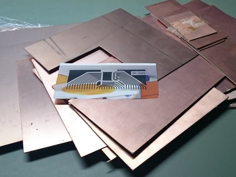
3. cutting laminate
Choose copper clad laminate sheet to cut from. I have plenty of single and 2-sided FR4 sheets from 1.0 to 1.6 mm of thickness. Usually I do not care, sometimes (for microwave specs) I design board for exact thickness.
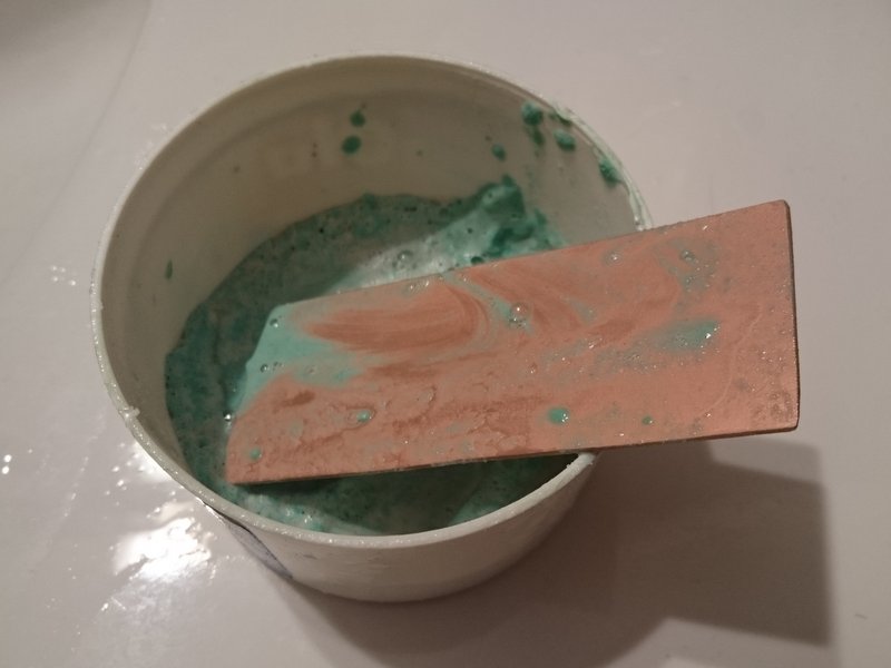
4. cleaning copper
Stored copper clad laminate is oxidatex and coated with dirt, fat etc. Cleaning is required to help copper etching. Some use sandpaper and isopropyl alcohol, I stict to kitchen abrasive paste. Avoid touching cleaned surface with oily fingertips, otherwise etching will be less effective and requires longer processing that may cause overetching.
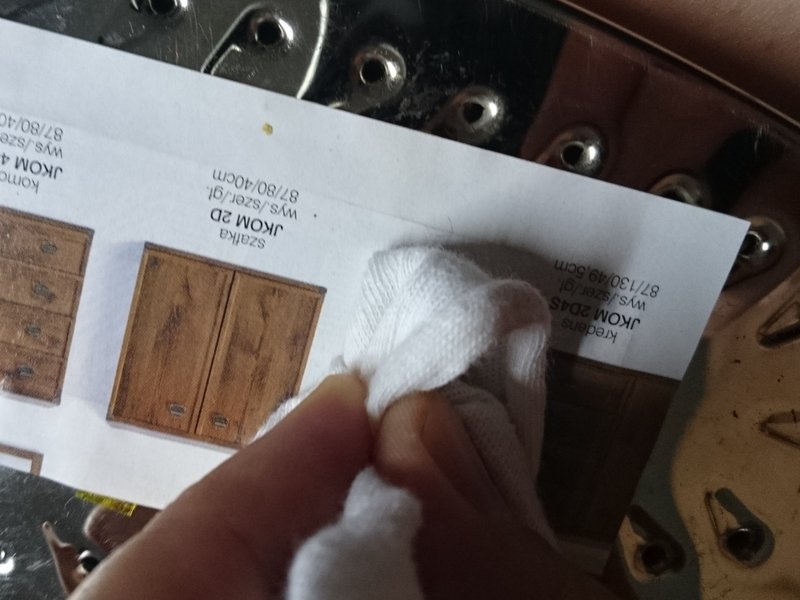
5. heating
Stick printout to copper layer of laminate. I use thermoresistive kapton tape for precise placement. Board is heated on iron set upside-down with 3/4 of max power for 40-60 seconds. For larger boards it takes a bit longer. First I warm up paper-up to warm up board evenly, then I turn it upside down.
6. bonding toner
Make sure toner is well-bonded to copper. I make round moves using cloth pressing slightly every piece of print to the board. Pay special attention to corners and edges. Lack of good bonding leads to unwanted effect: toner stays on scrapped chalk paper (see step 8). Do not overpress either: melted toner will squize too much and traces will deform making shorts in worst case.
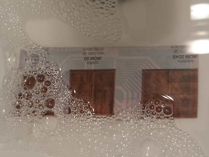
7. soaking paper
Paper must be removed in a way that toner remains on copper. The best way is to soak it in warm water with addition of soap or dishwashing liquid. Some people claim that adding vinegar helps as it reacts with chalk making paper more britle and easier to let go.
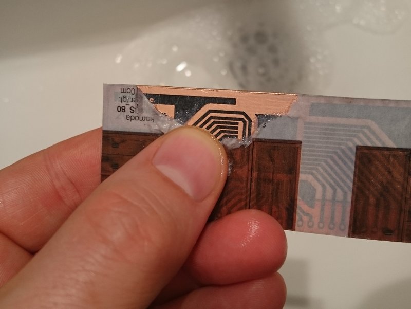
8. scrapping paper
The thinner paper is used the shorter soaking time is required. Within 5-15 minutes paper can be scrapped by delicate rolling using thumbs. Some threads of paper can be glued to toner bonded to copper; do not bother too much, it does not prevent etching solution from dissolving copper.
Note that steps 6-7-8 can be simplified using special toner transfer paper that does not require soaking. Such paper can be either purchased or made at home (creating dextrine from corn starch). I do not care about super precise results so tested chalk paper is good enough.
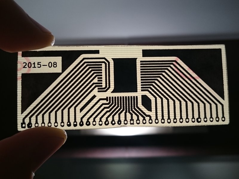
9. reviewing transferred toner
Dry board after paper removal. Look for irregularities introduced by dust particles between toner and copper or weakly stuck toner.
10. fixing irregularities
White spots or broken traces can be fixed with permanent marker. I prefer oil marker that is more resistive to etching solution.
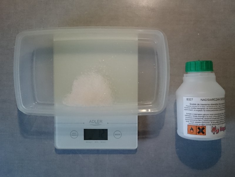
11. preparing chemicals
Prepare etching solution like most popular sodium persulfate. Some people keep it in liquid form for reuse. Since I rarely manufacture PCBs I prefer dissolving it on the fly: based on etched area I prepare rounded amount of Na2S2O8 required (about 1.5g per each 10x10mm of copper to be consumed) and dissolve in hot distilled water.
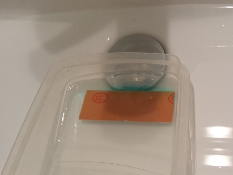
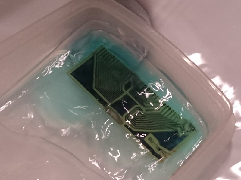
12. etching
Etching is done in plastic box sinked in larger basin with hot water that I can replace if cooled down. This way solution keeps high temperature speeding up chemical process.
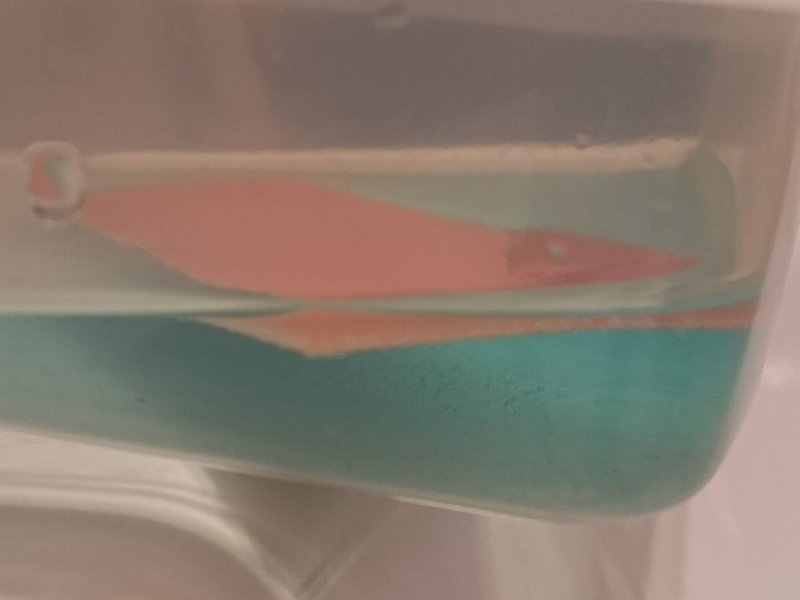
13. etching by floating
Single side PCB can be carefully placed on surface so it floats – this way reaction byproducts (salt) goes down and etching does not slow down. This is good way to leave board unattended, checking from time to time (every 5 minutes) state of completion.
15. etching by flushing
Fastest way of pickling is to swing the box mixing the solution constantly. Be careful as the soultion can be easily spilled out and copper sulfates produced are toxic.
Warning: flushing byproducts in toilet is irresponsible! Small amounts can be disposed after neutralization by applying aluminum, and later baking soda as described here applying necessary safety measures.
15. control
Etched board is flushed with tap water and quality controlled. Copper must be toner covered otherwise further etching is necessary.
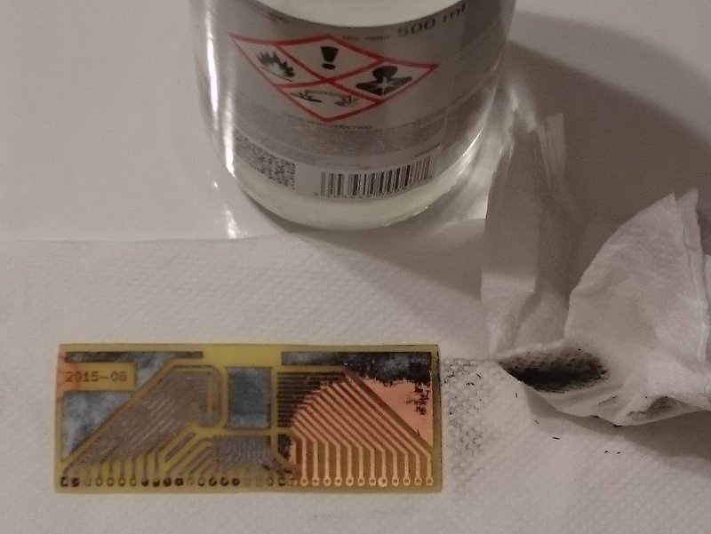
16. removing toner
Toner can be removed mechanically (polishing paste) or chemically using paint thinners like acetone or toluene. I prefer the latter as it takes less than a minute to competely remove copper mask.
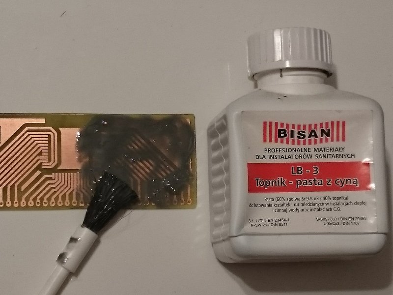
17. tin paste coating
Last stage is coating PCB with antioxidation layer that makes soldering easier task. Old style technique was to use resin solution. Long drying time and organic compounds were disadvantageous however. Clever trick is to use tin paste for plumbers used to solder copper pipes. Only copper areas of PCB must be painted.
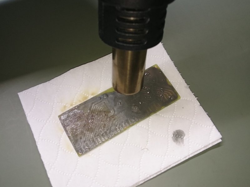
18. baking tin paste
Plumbers tin paste must be baked. Since paste creates chemical vapors do not use baking oven 🙂 Few minutes with hot-air gun turns paste matt which means it is ready.

19. control
PCB is flushed again in tap water and tin paste remains are removed. If coating (step 17) did not cover important areas patches of tin paste can be applied again.
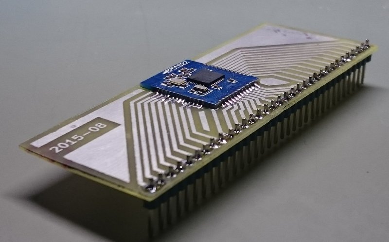
20. soldering
Finally drilling and soldering happens and proto-board can be connected to bread board for experiments when time permits.


Going from idea to schematic to printed PCB” could be easily realized through https://ZZZZZ.com which is free tool for schematic capture, spice simulation, PCB design.
ZZZZZ is very good tool for developing circuit and PCB. It helps you complete the process from schematics to the finished PCB in the shortest time, high quality manufacturing, competitive price PCB prototype service and you could track this link to order https://ZZZZZ.com/order
I do not accept ads here, wiping out advertised product name…