
Close GSM antenna proximity to bare PCB was troublesome latching microSD. Using most resilient flash cards nearly solved the problem. Extra shielding would help to prepare for worst field conditions like area of weakest GSM signal leading to highest emission and EMI. I took long and tough lesson to get shielding done right.
Initially I tried to isolate L-shaped PCBs from antenna with L-shaped aluminum foil sheet in between. Running system in open air was fine. As soon as I placed PCBs it in metal box SD started failing instantly on data transmission. Half an hour of play with different shapes of foil (glued to paper to avoid accidental shorting) I got nowhere – because of reflections signal was freely penetrating PCBs thru holes.
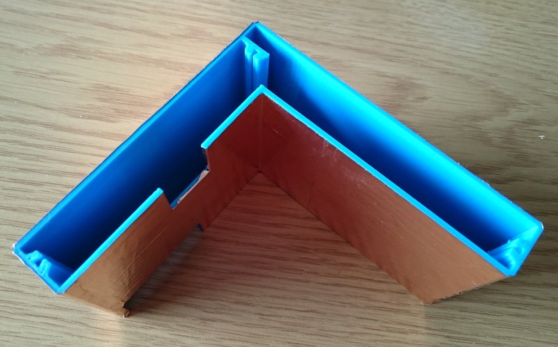
First 3D printed shielding
Shield sliding on PCBs
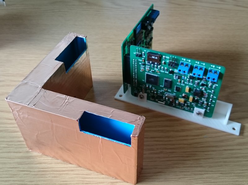
First systematic approach was to print on 3D printer L-shaped box with largest possible coverage for both PCBs. The idea was
to have this box detachable without disassembling logger inner frame disconnecting cables only. There were two holes for wires plus opened bottom. Printed box was wrapped with sticky copper foil and mounted for test in metal box to simply fail. I had high hope it would at least perform a little better. Hours of OpenSCAD design and printing landed in trash bin.
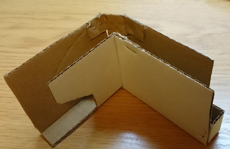
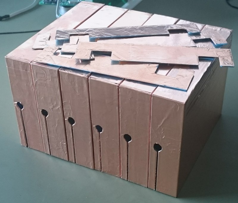
Cardbord fast prototyping

First shielding tests failed
Then I stepped back to cardboard and aluminum foil. It is faster to cut and glue and then to reshape for subsequent tests if needed. Test by test I decided to make it shorter, still L-shaped yet covering only main board (microSD) and 1/3 of board wiht GSM. Results were so bad I was close to abandon shielding idea completely.
Last conspiracy theory crossing my mind was that EMI may come from inside – short trace of PCB between GSM module and IPEX antenna connector, or even the sharply angled antenna cable connected to second PCB board. I thought I could try to shield first PCB only, minimizing holes and slots. I imagined also that box could be added or removed without touching wires – cables can be slide thru tinny slit alongside, neat an clean approach. The other side tightly matches pin header socket leaving only 5x20mm of uncovered window below the connector. This time I got bottom side cap thought to be glued to PCB mounting frame. Box covered by aluminum foil was assembled for tests, fragile Samsung microSD mounted, PCBs placed in metal box, system started and… worked!
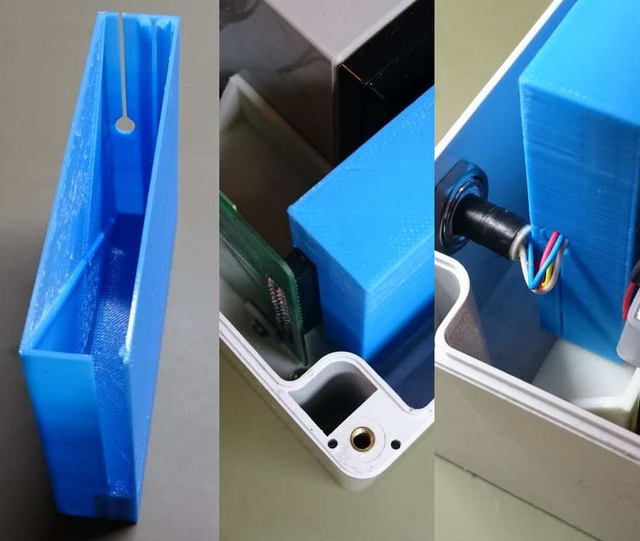
Tight easy-mount shielding
Faraday’s cage for field testing
Shields serial home production
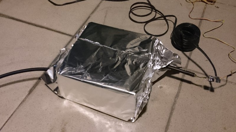
Few tests later aluminum kitchen foil was replaced with copper foil as it is performing better from mechanical and electromagnetic perspectives. The whole logger box was reassembled and wrapped with large sheet of aluminum again – this time aluminum was used to simulate metal box conditions in the field, equivalent of integration test in IT. Firmware was compiled to transmit data 10 times faster to push system into trouble as soon as possible. Two days later (equivalent of 3 regular weeks) it was still running ok even hosting fragile Samsung microSD inside.
And again, I have lost dozen of work-hours to gain ton of respect to physics running microelectronics world.
See also other related articles:
[posts_by_tag tag=”WLS”]


